Forgot Password?
Mobile number is now mandatory for the security of your account.
We've sent you a verification code on your mobile number. Please enter it here to set a new password.
We've sent you a verification code on your mobile number or email address. Please enter it here to set a new password.
a). Explain the fabrication steps of CMOS inverter in p-well CMOS technology.
b) Draw the circuit of function using
i) Transmission Gate
ii) Pseudo Logic
b} Explain CMOS logic based NAND SR latch circuit and explain its working.
b) Describe the operation of basic MOS inverter. Derive the expression for pull-up to pull down ratio for a CMOS inverter.
a) Explain the MOS structure with N-type substrate in Accumulation,Depletion and inversion regions with the help of energy band diagram.
b) Find the threshold voltage and body factory for a N-channel transistor with n+ silicon gate if tor 200 AO, NA=3x 10%/cm, gate doping NU=4x10¹⁹/cm3 and positively charged ions at the oxide silicon interface per unit area is 1010/cm2, T=300 K.
a) Obtain equation of delay for CMOS inverter driving load CL .
b) Draw the stick diagram of i) X-NOR Gate ii) 2:1 MUX.
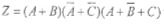
a) Design the circuit described by the function using CMOS logic. Also find the equivalent CMOS inverter circuit if (W/L)p=10 and (W/L)n=5.
a) Draw and explain negative edge triggered D flip flop and verify it.
a) Explain the advantages of dynamic logic circuit over static logic circuit.Explain Domino and NORA CMOS logic circuit with suitable example.
b) Draw and explain TSPC-based negative edge triggered DFF.
a) Discuss the hierarchy of various semiconductor technologies with Moorey'slaw and VLSI design flow (Y chart).
b) Explain the following circuits
.i) Variable threshold CMOS circuit
ii) Multiple threshold CMOS circuit
Short note:
a) MOSFET Scaling
b) Concept of regularity, Modularity and Locality
a) Explain MOSFET capacitance model with the help of suitable diagram.
b) Draw and explain the layout of CMOS inverter, follow all based rules.
C) Explain body effect and flat band voltage with the help of suitable diagrams.
d) Discuss how charge sharing problem can be avoided in dynamic CMOS logicstyle.
e) Explain why substrate and well contacts are important in CMOS.
Congratulations! Your trial of
is now active.
Let's catch up on a Zoom call and I'll help you craft a killer career plan! Bring your own coffee.
Sourabh Bajaj


 using
using for a N-channel transistor with n+ silicon gate if tor 200 AO, N
 for CMOS inverter driving load CL .
 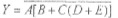 using CMOS logic. Also find the equivalent CMOS inverter circuit if (W/L)p=10 and
(W/L)
using CMOS logic. Also find the equivalent CMOS inverter circuit if (W/L)p=10 and
(W/L) based rules.