Forgot Password?
Mobile number is now mandatory for the security of your account.
We've sent you a verification code on your mobile number. Please enter it here to set a new password.
We've sent you a verification code on your mobile number or email address. Please enter it here to set a new password.
a. Design full adder and draw the circuit using two input NAND gates.
Explain the following canonical form:
ii) F(x, y, z) = (x + 2)(x+y)(y +z)
b. Find the minimal POS expression of incompletely specified Boolean function using K-map ,f(a, b, c, d) - M(1, 2, 3, 4, 9, 10) + d(0, 14, 15).
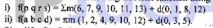
C. Find all the minimal SOP expression of f(a, b, c, d) - (6, 7, 9, 10, 13) + d(1, 4, 5, 11, 1) using k-map.
a. Find all the prime implicants of the function:
f(a, b, c, d) = (7, 9, 12, 13, 14, 15+ d(4, 11) using Quine - MaClusky's algorithm.
(LU Marksb. For a given incomplete Boolearn function, find a minimal sum and minimal product expression using MEV technique taking least significant bit as map entered variable. f(a, b,c,d) = (1, 5, 6, 7,971, 12, 13) + d(0, 3, 4).
a. Implement the function using active low output dual 2 : 4 line decoder IC74139
i) f1(A, B, C) = m(0, 1, 2, 5)
ii) f2(A, B,C) =M(1, 3, 4, 7).
b. Design priority encoder with three inputs, with middle bit at highest priority encoding to 10,most significant bit at next priority encoding to 11 and least significant at least priority ending 01.
a. Define multiplexer and demulitplexer and draw block diagram.
b. Design 4 : 1 multiplexer, draw the circuit using gates.
c. Explain how will you implement the following function using implementation table,F(A, B, C, D) = m(0, 1, 3, 4, 7, 10, 12, 14) with A, B, C as select lines.
a. Explain the following canonical form:
i) F(x, y, z) =
b.Design and draw the circuit of look ahead carry generator using gates. Draw the block diagram of 4-bit parallel adder using look ahead carry generator.
c. Design single bit magnitude comparator and draw the circuit.
a. Obtain the following for SR flip-flop:
i) Characteristic equation
ii) Excitation table
iii) State diagram.
b. With the help of a schematic diagram, explain how a serial shift register can be transformed into a i) ring counter ii) Johnson counter.
c. Design mod6 synchronous counter using D-flip-flops.
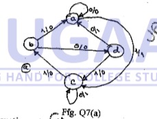
a. A sequential network has one input and one output the state diagram is shown in Fig. 7(a).Design the sequential circuit using T flip-flops.
(a)Derive the transition equations, transition table, state table and state diagram for the following:
Write notes on:
a. Mealy and Moore model
b. State machine notation.
Design two 4-bit number serial adder.
Prove that symmetrical signal has a duty cycle of 50% and find the frequency, low and high duty cycles for asymmetrical signal if it is high for 3 ms and low for 4 ms.
Explain the structure of VHDL/Verilog program.
Find the SOP of the following Boolean function using K-map :
Simplify f(A B C D) = m(0, 1, 2, 3, 5, 8, 12, 14, 15) using Quine - McClusky method.
Design a 16 : 1 multiplexer using two 8: 1 maultiplexers and one 2 : 1 multiplexers with expressions.
With relevant diagram explain n-bit magnitude comparator.
Give HDL implementation for 4 : 1 MUX using 'case statement.
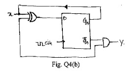
With state table and state transition diagram, analyse the behaviour of sequential circuit shown in Fig. Q4(b).
With a neat logic and timing diagram, explain the working of a 4-bit SISO register.
Name universal gates. Realize basic gates using NAND gate only.
Write verilog HDL code for 4-bit SIPO shift register.
Design synchronous modulus - 5 (mod -5) counter using JK - Flip-Flop.
Explain, design of 4-bit binary ripple - up counter using negative edge triggered JK -flip-flops with block diagram and timing diagram.
With neat diagram explain and compare Mealay and Moore machine.
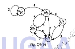
Reduce state transition diagram (Moore model) of Fig. 7(b) by i) Row elimination method ii) implication table method.
Discuss the two drawbacks of resistive divider used in converting D/A. Draw the schematic for a 4-bit binary ladder and explain how the digital to analog conversion is achieved using it.
Discuss the working of A/D converter:
ii) Counter type A/D.
i) Successive approximation A/D
What do you mean by characteristic equation of 'Flip-flop'? Draw the logic diagram, truth table and explain working of 'JK - Flip-Flop and implement the same using NAND gate.
Congratulations! Your trial of
is now active.
Let's catch up on a Zoom call and I'll help you craft a killer career plan! Bring your own coffee.
Sourabh Bajaj


 M(1, 2, 3, 4, 9, 10) +
  d(0, 14, 15).
  (6, 7, 9, 10, 13) +
  d(1, 4, 5, 11, 1) using k-map.
  (7, 9, 12, 13, 14, 15+
  d(4, 11) using Quine - MaClusky's algorithm.
  (1, 5, 6, 7,971, 12, 13) +
  d(0, 3, 4).
  m(0, 1, 2, 5)
 M(1, 3, 4, 7).
  m(0, 1, 3, 4, 7, 10, 12, 14) with A, B, C as select lines.
 m(0, 1, 2, 3, 5, 8, 12, 14, 15) using Quine - McClusky method.