Forgot Password?
Mobile number is now mandatory for the security of your account.
We've sent you a verification code on your mobile number. Please enter it here to set a new password.
We've sent you a verification code on your mobile number or email address. Please enter it here to set a new password.
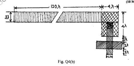
For the given multilayer structure shown in Fig. 04(b) calculate the total capacitance.
Write short note on :
iv) Built in self test (BIST)
iii) Level sensitive scan design and
ii) Test and Testability.
i) Input/output pads
Explain read and write operations in dynamic memory cell.
Describe the CMOS pseudo static memory cell with neat figure.
With neat figure explain transistor dynamic RAM cell.
Explain with neat diagram the 4x4 cross bar switch.
With the help of logic expressions explain how to implement arithmetic logio operations with a standard adder.
Explain with neat figure, non-inverting dynamic storage cells using CMOS transmission gate switch.
Draw and explain 4 : 1 MUX using transmission gate.
Obtain switch logic arrangements for (1) Vout - V1A + V2B + V3C using 3 way selector switch and (ii) 3 input nMOS OR gate.
Discuss latch-up in a p-well CMOS structure and its remedies. With neat figure explain twin tub CMOS process steps.
What are the most commonly used scaling models? Provide scaling factors for
(iv) speed power product
(iii) current density and
(ii) Gate delay
(i) power dissipation per gate
Draw and explain the basic structure of dynamic CMOS logic and discuss the charging sharing problem in this structure.
With neat circuit diagram explain :
(ii) An improved BiCMOS inverter with no static current flow and better output logic levels.
(i) A simple BiCMOS inverter
What do you mean by based design rule? Explain based design rules applicable to MOS layers and transistors.
Draw the CMOS circuit diagram, stick diagram and symbolic diagram of Boolean function F=
What are the uses of stick diagram? Give the table of color and monochrome stick encoding for simple single metal NMOS process.
Deduce an equation for figure of merit of MOS transistor. Fnd the operating frequency fo in the following condition = 125cm2/v-sec, L=2 m, Vgs = 2V and What = IV.
For an NMOSFET, the following details are available n = 500cm2/V-se, (Va - Vin) = 2.6V tox = 100 Å. Calculate Rn of the device if w 100m L = 0.5m
Congratulations! Your trial of
is now active.
Let's catch up on a Zoom call and I'll help you craft a killer career plan! Bring your own coffee.
Sourabh Bajaj


 based design rule? Explain
  based design rules applicable to MOS layers and transistors.
 = 125cm2/v-sec, L=2
  m, Vgs = 2V and What
  = IV.
= IV. n = 500cm2/V-se, (Va - Vin) = 2.6V tox = 100 Å. Calculate Rn of the device if w 100
 m L = 0.5
 m
m