Forgot Password?
Mobile number is now mandatory for the security of your account.
We've sent you a verification code on your mobile number. Please enter it here to set a new password.
We've sent you a verification code on your mobile number or email address. Please enter it here to set a new password.
What do you mean by Q notations used in DSP algorithm implementation? What are the values represented by 16 bit numbers N-4000h, in Q15. Q7 and Q0 notations?
Describe with a suitable diagram a digital model for production of speech signal.
Explain the operation of pulse position modulation (PPM) to encode two biomedical signals.
Explain with a neat diagram, the synchronous serial interface between the C54XX and a CODEC device,
What are interrupts? How interrupts are handled by the CS4XX DSP processor?
Design an interface to connect a 64k x 16 flash memory to a TMS320C54XX device. The processor address bus is Ao to A15 .
Draw the I/o interface timing diagram for read-write-read sequence of operation.
Determine optimum souling factor to prevent over flow.
Explain an 8-point DIT-DFT implementation structure based on the butterfly on the TMS320C54XX.
Why zero padding is done before computing the DFT?
With the help of block diagram, explain the implementation of an FIR filter in TMS320C54XX processor. Show the memory organization for the filter implementation.
Write an assembly language program for TMS32054XX processor to multiply two Q15 numbers to produce Q15 result.
An analog signal is sampled at the rate of 8 KHz, if 512 samples of the signal are used to compute DFT, X(k), determine the analog and digital frequency spacing between adjacent X(k) elements. Also determent analog and digital frequencies corresponding to k = 64.
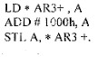
By means of a figure, show the pipeline operation of the following sequence of TMS 320C54XX instruction. Assume initial value of AR3 is 80h and the values, stored in memory locations 80, 81h, 82h as 1, 2 and 3
Differentiate between MAC and MACD instruction by way of explaining them.
Explain the operation of serial input/outputs ports and hard ware timer of TMS320CS4XX on chip peripherals.
Consider that AR3 is selected as the pointer for the circular buffer. The various register contents are Bkn= 40, AR3 = 1020H, ARO = 0025H. Find : i) start and end address of the buffer ii) contents of AR3 after the execution of the instruction LD +AR3(121)% iii) conterts of AR3 after the instruction LD • AR3 +0%.
Describe the multiplice/address unit of TMS320C54XX processor with a neat block diagrain.
Compare architectural features of TMS320C25 and motarala fixed point DSP devices.
With a neat block diagram, explain address generation unit of DSP system.
Briefly explain about the 4x4 Braun multiplier with its structure. In nxn structure how many adders are required? n parallel multiplier
With a neat block diagram explain about the saturation logic and its use.
Explain the decimation and interpolation with equation. Ler x(n) = [3, 2, -2, 0, 7). It is interpolated using an interpolation filter bk = (0.5, 1, 0.5] with interpolation factor-2. Determine the interpolacion sequence.
List the major architectural features used in DSP system to achieve..high speed program execution.
Congratulations! Your trial of
is now active.
Let's catch up on a Zoom call and I'll help you craft a killer career plan! Bring your own coffee.
Sourabh Bajaj