Forgot Password?
Mobile number is now mandatory for the security of your account.
We've sent you a verification code on your mobile number. Please enter it here to set a new password.
We've sent you a verification code on your mobile number or email address. Please enter it here to set a new password.
a. Explain the need of cascade amplifier and list the advantage of this Circuit.
c. For common gate amplifier as shown in Fig 08.(c), gm = 2.8ms, rd =50 Calculate zs, zo, and Av.
b. With equivalent model of JFET common drain configuration. Obtain the expression for zi, zo and Av.
a. Define transconductance gm and derive expression for gm.
c. With neat circuit explain the working of series resonant crystal oscillator. A crystal has L =0.1H ,C =0.01 pF find the series resonating frequency.
ii) Design the value of an inductor to be used in Colpitts oscillator to generate a frequency of 10MHz. The circuit is used a value of C1 =100pF and C2 = 50pF.
b. i) The frequency sensitive arms of the wien bridge oscillator uses C1 = C2 =0.001 and R1 = White R2 is kept variable. The frequency is to be varied from 10KHz to 50KHz by varying R. Find the minimum and maximum values of R2.
a. With neat circuit diagram explain the operation of BJT Hartley oscillator.
c. What is Harmonic distortion? Calculate the harmonic distortion components for an output signal having fundamental amplitude of 2.5V second harmonic amplitude of 0.25V, third harmonic amplitude of 0.1 V and Fourth harmonic amplitude of 0.O5V. Also calculate the total harmonic distortion.
b. Draw the circuit diagram of series fed directly coupled Class - A amplifier. Give the expression for dc power input and ac power output and show that efficiency is 25%.
a. Draw input and output wave forms of Class A, Class-B and Class - based on the location of Q-point, and briefly discuss.
6. Derive the expression for input resistance ( Rif)for voltage series feedback amplifier .
b. With block diagram, explain the concept of feedback List the advantages of negative feedback.
a. Explain Reverse recovery time of a semiconductor diode.
c. Draw and explain frequency response of an amplifier and briefly discuss the effect of various capacitors on frequency response.
b. Describe miller effect and derive an equation for miller input and output capacitance.
a. An amplifier consists of 3 identical stages in cascade; the bandwidth of overall amplifier extends from 20Hz to 20kHz. Calculate the band width of Individual stage.
c. Using h-parameter model for a transistor in C.E configuration. Derive expressions for Ai, zi and Av.
b. Derive an expression for zi, zo, Av and Ai of a CE fixed bias configuration using re model.
a. For common base configuration shown in Fig Q3(a). Find res, zs, zo, and Av.
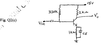
c. For the circuit shown in Fig. 02(c). Find IS, IC, VCE. VC and VE Assume = 100,VBE =0.7.
b. Derive the expression for lS, VCE and S(ICO) for voltage divider bias using exact analysis.
a. What is transistor biasing? Discuss the causes of bias instability in a transistor.
c. What is clamper circuit? Explain the operation of Positive and Negative clamper circuits and draw the wave form. [Assume Ideal Diode).
b. The Fig. QI (b) shows two way clipper. Determine its output wave form. Assume diode drop of 0.7V.
Congratulations! Your trial of
is now active.
Let's catch up on a Zoom call and I'll help you craft a killer career plan! Bring your own coffee.
Sourabh Bajaj


 Calculate zs, zo, and Av.
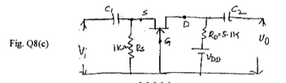
 and
R1 =
and
R1 =  White R2 is kept variable. The frequency is to be varied from 10KHz to
50KHz by varying R. Find the minimum and maximum values of R2.
White R2 is kept variable. The frequency is to be varied from 10KHz to
50KHz by varying R. Find the minimum and maximum values of R2. 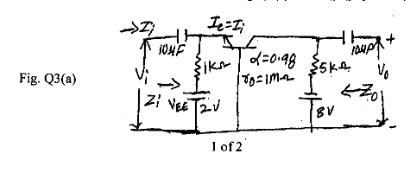
 = 100,VBE =0.7.